


JFET (junction field effect transistor)
JFET:The junction gate field-effect transistor is a earliest type of field-effect transistor. It can be used as an electronically-controlled switch or as a voltage-controlled resistance.
Types: 1. N channel , 2. P channel
Since electron have higher mobility than holes ,the n channel JFET provide higher conductivity and high speed and preffered in most application to the p-channel JFET.
N Channel JFET
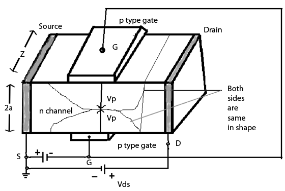
Structure : The n type material is sandwiched between two highly doped layer of p-type material that is designated p+.This type of device is called an n channel JFET.
The two p type regions in the n-channel JFET shown in figure are reffered to as the gate.
Each end of the n channel is joined by a mettalic contact in accordance. With the direction of baising voltage as shown in figure left hand contact which supplies the source of following electron is reffered to as the source,where as which drains the electrons is called the drain.
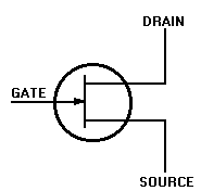
The circuit symbol for an n channel JFET as shown in figure.
For a p channel JFET. the polarites of the two baising voltage Vg and Vd are interchanged.
P.O.O (principle of operation): Principle is quite simple.
1. Under normal operation condition
Vg (gate voltage) - 0
Id (Drain voltage) - 0
The channel b/w Gate junction entirly open
2. When small voltage Vd is applied b/w the drain & source, the n-type semiconductor bar act as a simple resistor and current Id increases linearly with Vd.
3. If a reverse gate voltage Vg is applied across the p-n junction the majority of free electrons are depleted from the channel.
4.As the drain voltage Vd is further increased, the space charge region expand and joined together,so all free electrons carrier are complet depleted in the joined region.Thiscondition is called pinch off
5. When channel is pinch off , the drain current Id remains almost constant,but drain voltage contineously increases.
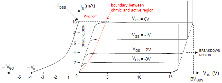
Pinch off Voltage (Vp): The pinch off voltage is the gate reverse voltage that removes all the free charge from the channel.